Electron beam lithography (EBL) is today one of the key fabrication techniques for structuring at the nanoscale. Born in the late 1960s by modifying the design of scanning electron microscopes (SEMs), its operating principle is relatively simple: a focused electron beam is scanned on a substrate covered by an electron-sensitive material (resist). This causes the change of its solubility in suitable solvent or developments, based on the energy deposited by the electron beam for which there is the selective removal of the exposed areas for the positive resistors, or not exposed for the negative ones. Since the discovery of polymethylmethacrylate (PMMA) as a resist electron by Hatzakis in 1969, EBL has become one of the leading techniques for making a wide variety of devices, ranging from integrated circuits, to photonic crystals, to NEMS.
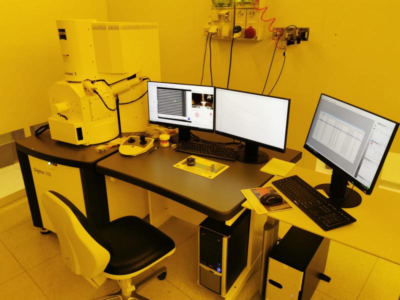
The system that was acquired by IOM for the nano fabrication facility starts from the same concept from which these tools were born, namely the use of a normal FE-SEM to generate very high resolution nanostructures. The main difference between a SEM and an EBL is in fact minimal: if in a SEM the beam is scanned on the sample to collect electrons emitted to form an image, in an EBL the same beam is "guided" by a pattern generator to expose only the areas of interest.
The SEM in question is a latest generation FESEM, the ZEISS SIGMA 300. Based on the proven Gemini technology, it allows to reach very high resolutions even using very low acceleration voltages, thanks to the possibility of having small probes and high signal ratios. noise.
Equipped with SE and Inlens detectors, the sigma 300 employs Accelerating Voltage between 0.02 - 30 kV.
As for the pattern generator, it is a proven and state-of-the art RAITH Elphy Quantum. Here are some of the features:
• 6 MHz dual DAC addressing
• 2 high speed 16-bit DACs for X and Y main beam deflection for overlap alignment and write range calibration
• beamblanker control circuit TTL 5V