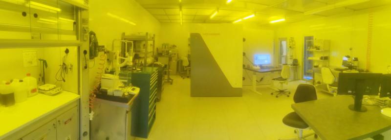
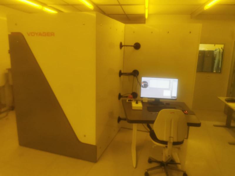
Installation of the new RAITH EBL system completed at our Nano Fabrication Facility (FNF) @ IOM.
The RAITH VOYAGER system, acquired thanks to the project STRADA, is a high-performance solution for electron beam lithography, designed to ensure nanometric precision and operational flexibility.
Key Features
The electron column operates with a beam energy adjustable between 50 and 100 kV, and beam currents ranging from 50 pA to at least 40 nA, providing high versatility and ultra-stable current performance, with fluctuations of less than 0.2% per hour. The electron source is field emission (FEG), and the system includes electrostatic beam deflection along with a tail-free beam blanker for optimal beam control at the crossover point.
The system achieves a resolution below 8 nm, with a writing field up to 500 µm (at 50 kV). Stitching accuracy in Step&Repeat (S&R) mode is 30 nm or better, while overlay error between consecutive layers does not exceed 25 nm. The system also features real-time dynamic correction for focus, astigmatism, and distortion.
The pattern generator operates at a 50 MHz clock, with a 20-bit DAC and upgradable firmware, supporting three writing modes:
-
Algorithmic writing, with direct loading of binary files generated by custom algorithms—ideal for complex structures such as large-area metalenses;
-
Stitch Error Free (S_E_F) writing, for repetitive pattern exposure over large areas (more than 5 mm × 100 µm) without stitching artifacts;
-
Writing on pre-identified zones, using ex-situ images from optical or electron microscopy.
The control software is comprehensive and fully integrated, offering features such as:
-
CAD data import/export, editing, and optimization;
-
Proximity Effect Correction (PEC);
-
Automated process control (autofocus, autostigmator, brightness, contrast);
-
Automated metrology;
-
Pre-optimized exposure modes for either high resolution or high throughput;
-
Automatic dwell time determination.
The positioning system includes an XY stage with laser interferometric control, hybrid stepper-piezo actuation, and a minimum positioning resolution of 2 nm. The Z-axis has a travel range of at least 15 mm, supporting substrates up to 12 mm thick.
Among the advanced software options, the system includes Periodixx and Algorithmixx licenses, specifically designed for the design and optimization of complex nanophotonic structures.