Minimization of contamination associated with the graphene transfer process from the growth substrate to the device surface is a major requirement for large scale CVD graphene device applications. We performed a polymer-free method of commercial CVD-grown graphene transfer from the initial copper substrate to the silicon device: 15 nm-thick titanium layer replaces completely the polymer (PMMA) film as supporting layer during the transfer process. The approach reduces significantly the level of contaminations for supported and suspended graphene layers. Raman spectroscopy proves the quality of the transferred graphene, while X-ray photoelectron spectroscopy and X-ray absorption spectroscopy were used to assess the amount of the contaminants left by the transfer process. Overall carbon contamination was reduced by a factor 2, while contaminations originating from the metal etching in hydrofluoric acid, namely titanium and fluorine, were absent within the sensitivity of the used techniques.
2016 Carbon 103, pp. 305-310
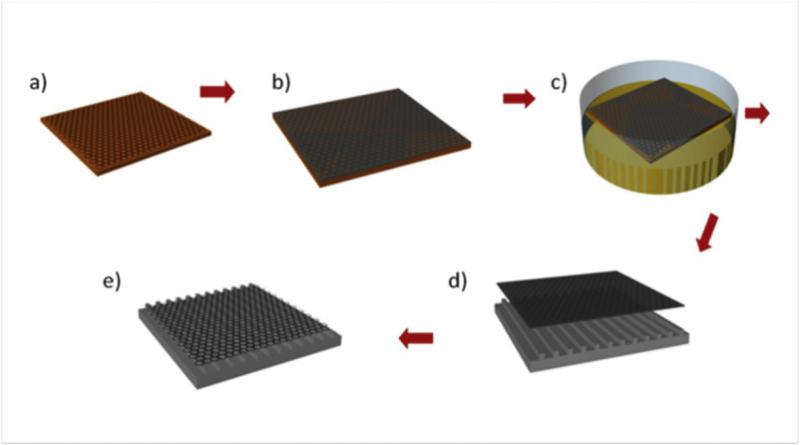
The transfer process
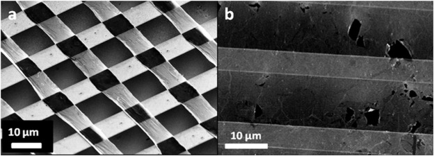
SEM images of suspended graphene
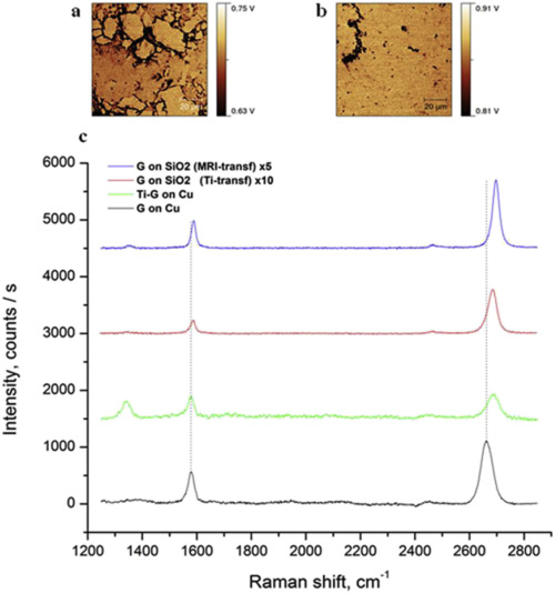
LSC images of (a) PG sample and (b) MG sample. The dark parts indicate areas in which graphene is rolled up or in which defects or contamination are present, indicating that Ti-transfer produces a more uniform graphene layer; (c) Raman spectra of as-grown graphene acquired directly on Cu foil (black), covered by 15 nm thick Ti layer (green), and transferred on SiOx/Si substrate using Ti (red) or mr-I 7020 (blue).
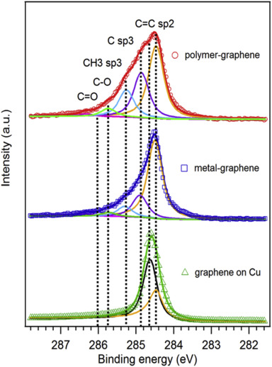
C1s XPS spectra of PG (red curve), MG (blue curve) and graphene on Cu as grown (green curve).