Papers

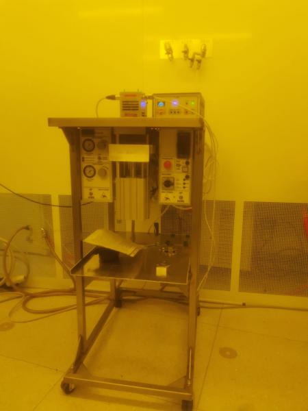
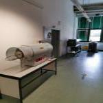
We are excited to announce the availability of a brand-new UV Nanoimprint Lithography (UV-NIL) system at the FNF.

UV-NIL.jpg

This fully custom system was entirely designed and built in-house at our institute, showcasing the synergy between mechanical, electronic, and nanofabrication expertise. The setup includes a semi-automated pneumatic press capable of imprinting substrates up to 3 inches in diameter.

We are pleased to announce that the FNF technical team is expanding with the addition of Dr. Luca Sbuelz.

Luca earned his PhD at the University of Trieste, conducting research in a joint laboratory between the University and Elettra-Sincrotrone Trieste. His doctoral work focused on the commissioning of a mass-selected atomic cluster source and its application in the deposition and characterization of mass-selected clusters on two-dimensional materials, primarily graphene epitaxially grown on various substrates.

We are pleased to announce a renewal in the Management Board of the FNF Facility. Dr. Daniele Ercolani has joined the board, taking over from Dr. Dan Cojoc. We extend our heartfelt thanks to Dan for his invaluable contributions over the years, and we warmly welcome Daniele to his new role. We look forward to continuing to grow and improve our Facility together.

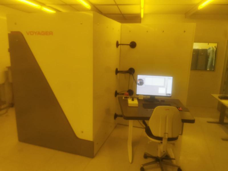
Installation of the new RAITH EBL system completed at our Nano Fabrication Facility (FNF) @ IOM.

The RAITH VOYAGER system, acquired thanks to the project STRADA, is a high-performance solution for electron beam lithography, designed to ensure nanometric precision and operational flexibility.

Voyager.jpg

A significant challenge in graphene fabrication is the production of large, suspended graphene layers. This issue applies to any kind of graphene-based device and is particularly critical when the fabrication of closed cells is required, for example in the fabrication of large, sealed cells for in-operando XPS or TEM investigation, or the fabrication of Golay cell-like bolometers.

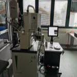
The new FNF SEM-FIB laboratory is ready!
The room houses the Leo 1540XB cross-beam, SEM with Gemini column (acc. volt. 0.5-30 KV) and Orsay Physics Ga-ion FIB column. The system, integrated with the Quorum cryo stage (https://fnf.iom.cnr.it/new-cryostage-has-been-installed-cross-beam-fnf-l...), will also allow the investigation of biological samples and polymers, increasing the range of use of SEM and FIB.

Stanza forni

The spaces of the Nano Fabrication Facility are further enlarged: a new laboratory has been created for the facility, at the MM building, dedicated to tubular furnaces, for the oxidation processes of silicon and for the production of Glassy Carbon.
The maximum temperature of the furnaces is 1200 ° C; the gases available are currently O2, N2 and Ar.
Dry or wet oxidation modes are available for the oxidation of silicon.

A new Cryostage has been installed on the available Cross Beam at FNF labs; the tool will extend the fields of application of electron microscopy.

It should be noted that a new access mode to FNF will now be possible at a reduced rate, for those interested in accessing only the Dual Beam laboratory; in addition to this, the cryo stage, the sputter coater, the laminar flow hood for sample preparation, and finally the CO2 critical point drier system are also included.

In the framework of piezoelectric/ferromagnetic patterned heterostructures, the purpose of this work is to electrically control the magnetic properties by tuning the morphology, especially by modifying the magnetic shape anisotropy through patterned strain. We have thus designed and studied a heterostructure with bottom nano-striped and top full film electrodes. ZnO piezoelectric and CoFeB magnetic materials were chosen to respond at critical criteria of its geometry. In addition, numerical simulations and magnetostatic calculations were performed to understand the reproduction of the pattern across the multiferroic heterostructure. Calculations have shown that the geometry of the heterostructure presents strict constraints, as for instance the distance between stripes versus the piezoelectric thickness. This study is a preliminary step towards reversible patterning of magnetic properties.

Electrochemical sensors are devices able to determine the concentration, through direct electrical measurements, of molecules and biomolecules in solutions. The miniaturization to a size below the 1 um in small-size arrays of nanoelectrodes (NEA), offers advantages in terms of increased sensitivity and compactness. NEAs of nanoholes on a thin film of polycarbonate (PC) deposited on boron-doped diamond (BDD) macroelectrodes has successfully fabricated by thermal nanoimprint lithography (TNIL), with a high reliability and reproducibility.The device has employed for the detection of, gliadin protein fragments physisorbed on the polycarbonate surface of NEAs by immuno-indirect assay using a secondary antibody labelled with horseradish peroxidase (HRP), in the range of concentration of 0.5–10 g/mL, by cyclic voltammetry.The fabrication of high-resolution nanostructures allows low-cost production, and possibly the scale up of NEAs-based electrochemical sensing platform to monitor biochemical molecules for both food and biomedical applications.

Pages