In the framework of piezoelectric/ferromagnetic patterned heterostructures, the purpose of this work is to electrically control the magnetic properties by tuning the morphology, especially by modifying locally the magnetic shape anisotropy through patterned strain that would induce a reorientation of magnetization under bias along the stripe.
We have thus designed and studied a heterostructure with bottom nano-striped and top full film electrodes, as shown in Figure 1.
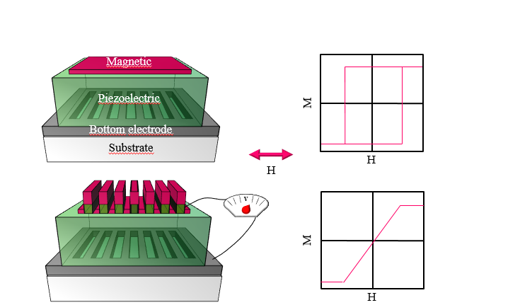

Figure 1. Sketch of the piezoelectric/ferromagnetic heterostructure without and with applied voltage (V). Besides each state, an example of magnetic hysteresis loop with different magnetic anisotropy is sketched.
After numerical simulations and magnetostatic calculations regarding the geometry and materials, we choose a geometry using first an insulating MgO (001) substrate of 5x5 mm2. On top of it, 10 nm thick Ag layer was deposited first with electron gun evaporators followed by 5 nm thick Ti layer to avoid any oxidization close to the piezoelectric film. Such thicknesses are required to have at the same time a continuous film with metallic properties, thin enough to minimize the roughness of the following piezoelectric film. Thereafter, a stripe pattern was designed by using laser interference lithography process. The stripe width and spacing was processed at 500 nm dimension (see figure 2) while the stripe length was done at 3 mm. The etching of this pattern was done by reactive ion etching. The Ti layer is first removed with a mix of reactive gases (CF4 (25sccm) and O2 (5sccm)), while inert Ar (30sccm) gas is used to etch Ag.
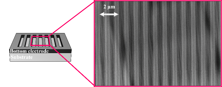

Figure 2. Sketch and SEM top view of a patterned stack on top of a MgO substrate with 500 nm metallic stripe width and spacing.
This study is a preliminary step towards reversible patterning of magnetic properties.